学习KEA之ADC之一:基本介绍
作者:曾Jerry 或 大橙员, 250359225@qq.com
学习KEA之ADC之一:基本介绍
学习KEA之ADC之二:查询方式
学习KEA之ADC之三:中断方式
学习KEA之ADC之四:FIFO
我们以KEA64系列来学习ADC, 其中KEA64系列包括:
- SKEAZN16AMLC®
- SKEAZN32AMLC®
- SKEAZN64AMLC®
- SKEAZN32AMLH®
- SKEAZN64AMLH®
其它系列的和KEA64类似,但也有点不同,具体要看各自的参考手册。
ADC特点
- Linear Successive Approximation algorithm with 8-, 10-, or 12-bit resolution
- Up to 16 external analog inputs(ADC0_SE0 ~ ADC0_SE15), external pin inputs, and 5 internal analog inputs, including internal bandgap(AD22), temperature sensor (AD23), and references
- Output formatted in 8-, 10-, or 12-bit right-justified unsigned format
- Single or Continuous Conversion (automatic return to idle after single conversion)
- Support up to eight result FIFO with selectable FIFO depth
- Configurable sample time and conversion speed/power
- Conversion complete flag and interrupt
- Input clock selectable from up to four sources
- Operation in Wait or Stop modes for lower noise operation
- Asynchronous clock source for lower noise operation
- Selectable asynchronous hardware conversion trigger
- Automatic compare with interrupt for less-than, or greater-than or equal-to,
programmable value
ADC框图

ADC时钟,由ADC_SC3 [ADICLK]选定:
- Bus clock
- Bus clock divided by 2
- Alternate clock (ALTCLK)
- Asynchronous clock (ADACK)
ADC寄存器

ADC的基本使用
KEA64的ADC是逐次逼近型ADC,最多具有16个外部模拟输入(ADC0_SE0 ~ ADC0_SE15)和5个内部模拟输入(包括温度传感器 (AD22)、内部带隙(AD23)和参考)。
ADC可以在任何可选通道上执行模数转换,可以转换成12位,10位或8位数字结果。转换完成后,结果将放置在数据寄存器(ADC_R)中,并设置转换完成标志ADC_SC1[COCO] = 1。如果使能了转换完成中断,则会产生一个中断ADC_SC1 [AIEN] = 1。
当在休眠期间或当ADC_SC1 [ADCH]位都为高电平时,ADC模块被禁用。
ADC的转换模式有:Single 或 Continuous Conversion (automatic return to idle after single conversion)
注意事项
It is recommended that the pin control register bit always be set
when using a pin as an analog input
- There is a 0.1 µF low-ESR capacitor from VREFH to VREFL.
- There is a 0.1 µF low-ESR capacitor from VDDA to VSSA.
- If inductive isolation is used from the primary supply, an additional 1 µF capacitor is placed from VDDA to VSSA.
- VSSA (and VREFL, if connected) is connected to VSS at a quiet point in the ground
- There is no I/O switching, input or output, on the MCU during the conversion
Bandgap(可作为其它ADC通道的参考源)
- 电压最小1.14 V, 典型1.16 V,最大 1.18 V
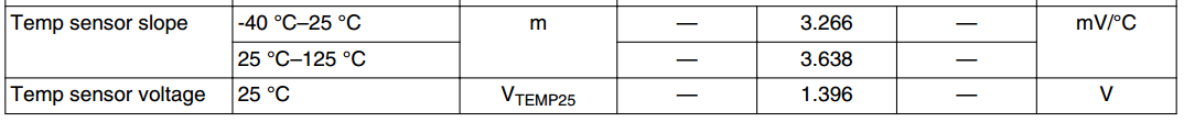
- Temp sensor voltage


还没有评论,来说两句吧...